Product
Power Amplifier

Technology Advantage
Finwave Power Amplifier products built with our proprietary GaN on Silicon technology improves on the superior performance of GaN solutions while adopting the cost and scale of manufacturing advantages from high volume CMOS silicon wafers.
Power Amplifier Product Technologies
Emode GaN-on-Si MISHEMT
3DGaN FinFET technology
Technology Advancements
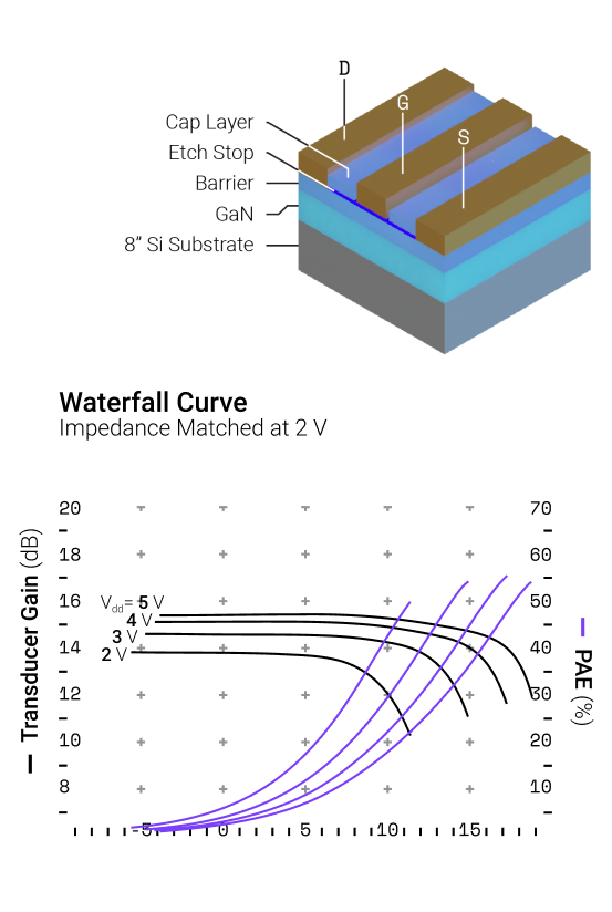
E-mode GaN MISHEMT Power Amplifier
Enabling Low Voltage, Single Supply Power Amplifier Solutions for 3GPP Bands
GaN-on-Si E-mode MISHEMT platform offers exceptional RF performance, delivering excellent gain and efficiency at easy to use, sub-5V voltages
- Etch-stop technology enables enhancement-mode with excellent RF performance.
- Low contact resistance enables envelope-tracking operation below 5 V for handset applications.
- MISHEMT technology for superior channel scalability for mmWave frequencies and beyond.
- 8" Wafer Silicon compatible process, scalable to 12" wafer size.


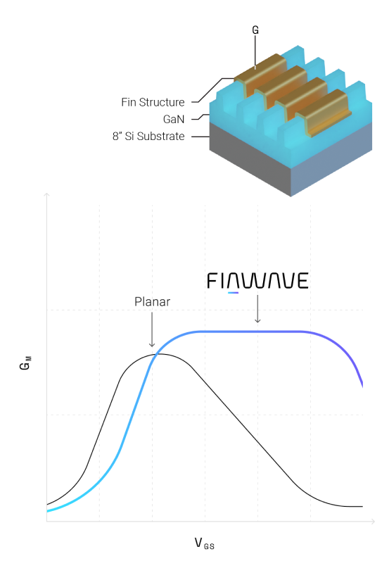
3DGaN FinFET Technology
Linearity Boost for Power Amplifiers
GaN-on-Si FinFET platform offers exceptional RF performance for Power Amplifiers of any size, significantly enhances power amplifier linearity, meeting the demands of advanced communication systems.
- Over 10dB linearity improvement with "multi-fin" technology.
- Excellent channel control for reduced leakage current.
- 8" Silicon wafer compatible process, scalable to 12" wafer size.
Comparison Chart
Features | Other Tech | GaN+ |
|---|---|---|
50% Efficiency improvement for identical EVM |  | |
GaN Performance with < 5.0 V Supply |  | |
Scalable CMOS compatible wafers and back-end |  | |
3DGaN FinFET technology for 10 dB linearity improvement |  |
With our unique GaN+ technology, proprietary 8” compatible manufacturing process and world-class expertise, our team at Finwave is poised to move entire industries forward and become the leading enabler of the 5G market.
References
- V. Johnson, Z. Pogrebin, M. Dipsey, H.S. Emmer, Y. Zhang, D.F. Pei and B. Lu, “200-mm enhancement-mode low-knee-voltage GaN-on-Si MISFETs for high-frequency handset applications,” CS MANTECH, 4.2.4, 2004.
- S. Joglekar, et. al. and T. Palacios, "Large signal linearity enhancement of AlGaN/GaN high electron mobility transistors by device-level Vt engineering for transconductance compensation," in IEEE International Electron Devices Meeting (IEDM) Dig., Dec. 2017, pp. 25.3.1-4.
- B. Lu, M. Sun and T. Palacios, "An etch-stop barrier structure for GaN high electron mobility transistors," IEEE Electron Device Letters, 34 (3), pp. 990-992, Mar. 2013.
- B. Lu, E. Matioli, and T. Palacios, "Tri-gate normally-off GaN Power MISFET," IEEE Electron Device Letters, 33 (3), pp. 360-362, Mar. 2012.
- D.S. Lee, et. al. and T. Palacios, "nanowire channel inAlGaN/GaN HEMTs with high linearity of gm and fT," IEEE Electron Device Letters, 34 (8), pp.969-971, Aug. 2013.